
| Home | S-100 Boards | History | New Boards | Software | Boards For Sale |
| Forum | Other Web Sites | News | Index |
.jpg) |
 |
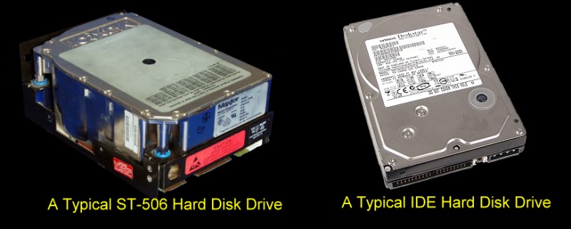
The IDE drive interface itself has a long history of incremental technical drive interface developments over the years. IDE evolved initially from Western Digitals hard drive interface used in the above IBM-AT. The central idea of the IDE interface was to place the drive controller, data separator etc. on the drive itself. This was a major improvement over the earlier ST-506 interfaces. It allowed for more drive construction possibilities, better standardization, better reliability and a more flexible connection to the computer itself. There were a number of improvements and name changes occurred over the years such as ATA/ATAPI. After the market introduction of Serial ATA in 2003, IDE/ATA interfaces were retroactively renamed Parallel ATA. I shall still use the term IDE here.
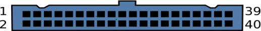
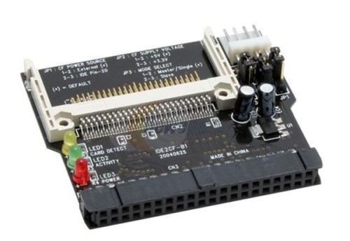
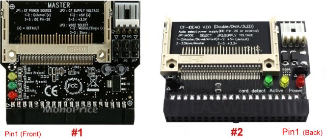
There are now actually two types of IDE connectors the "standard' 40 pin connector found on all IBM-PC type motherboards and a newer 44 pin connector used mainly in laptops for small laptop drives. The extra 4 pins are used to bring power (+5V) to the drive. Here is a picture of a standard IDE connector:-
Next install the two switches and only U2 and U3. We now will check port addressing. The board utilizes 74LS682's for port addressing. If your are unfamiliar with this technique click here.
Let’s assume you will be using the 4 port block 30H
to 33H. This is what I have the diagnostic software (MYIDE.ASM) port
defaults. We will set the 16 bit I/O address range to 00xxH by
jumpering K5 to 1-2 (the top two positions). Set switch SW2 positions 1-8 to
closed. Set
switch SW1 to 30-34H by having the switches (left to right):-
Open, closed, closed, open, open, closed, closed, closed.
Now put the card in your S-100 extender card and start the computer.
With your monitor at 0H in RAM enter:-
DB, 30, C3, 00, 00
Jump to 0H. With a probe you should have pin 19 of U2 pulse continuously.
Do not go further until you see this.
Next add all the other IC’s except the 8255, U7 and U9. Note, U4 MUST be
a 74H04 or 74S04 (see below). The board will not work with IDE/CF cards with
a 74LS04. (It seems to be OK for slower Hard Disks with a 74LS04 chip).
Repeat the above software test. Check that pin 1 & 19 of empty socket of U9
for a pulse. It should not pulse for any other value except 30H, 31H, 32H, & 33H.
This insures we are able to read the data port correctly. Now the write to
ports test.
Same software as above except we have:-
D3, 30, C3, 00, 00
Check for a pulse on pins 1 & 19 of empty socket U7. Again it should
not pulse for any other value except 30H, 31H, 32H, & 33H
Only if you get this to work go further.
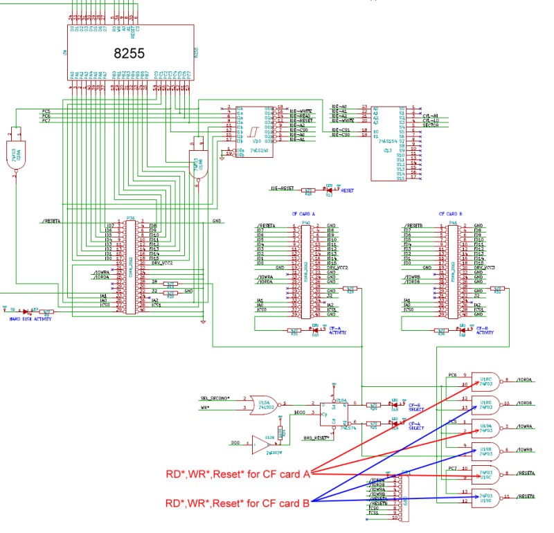
Insert the two 74LS244’s (U7 & U9) and the 8255.
We will now checkout the 8255. A complex chips with many configuration possibilities/modes. Fortunately for testing we need only the simplest mode where all 3 ports (A, B & C) are set as simple outputs. To do this from your monitor send to its control port (33H) the byte 80H. With this, port A (30H), port B (31H) and port C (32H) are configured for output ports.
With the LED’s on the board you can easily monitor port A.
Output to port C (32H), 0H. All the appropriate LED's should come on.
Then output 01, 02, 04, 08, 10H, 20H, 40H and 80H. The appropriate LED should
go off (see the above schematic).
Next we need to check port A (30H). Output to port 30H the value 0H. All the appropriate 8255 pins (4..1, 40..37) should be LOW. Then one at a time output a bit to this port. Starting at bit 0 send 01H to port 30H. See that pin 4 of the 8255 goes high. Continue all the way up to bit 7, pin 37 of the 8255.
Now do the same for the 8255 Port B (31H). First check the pins (18-25).
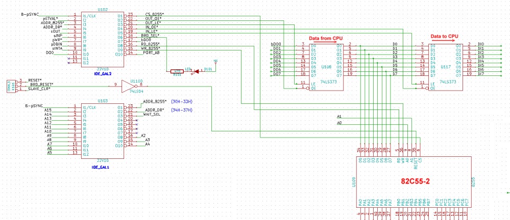
You will need a copy of the boards schematic. See
here.
Output to port 31H the value 0H. Pins 18-25 of the 8255 should be low. Output the
single bits pattern above and check each appropriate 8255 pin goes high.
Only if all of the above checks out should you go further.
Next we will check the actual IDE socket pins. Setup the 8255 to all ports
output as we did before (Output 80H to port 33H) then output to port 31H the
value 0H. ALL appropriate pins, 4,6…18 on any IDE socket should be 0. Then
output a 1 to port 31H. ONLY pin 4 on each IDE socket should be high. Same for all the other bits.
Only when you are sure that you can reliably output the correct bit pattern from
port 31H of the 8255 to any of the IDE sockets should you go further.
The boards are extremely well made so there is little chance of partial
etching. Any stuck bits are probably an error on your part.
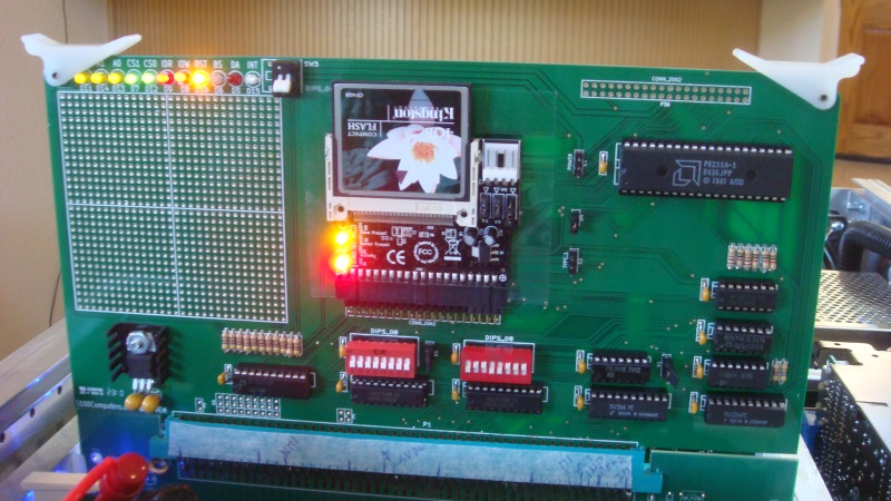
With the above completed, you are ready to fire things up with an IDE drive. I
have used the board with a number of drives and CF cards. I find it is
easiest to get things going with an old IDE hard drive. Be sure you plug
you plug the IDE cable in correctly. From the front of the board (V
regulators on left) the top IDE socket has pin 1 on the top row at the very
right back row of pins.
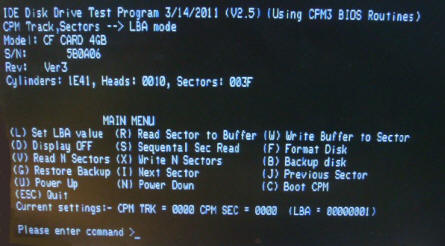
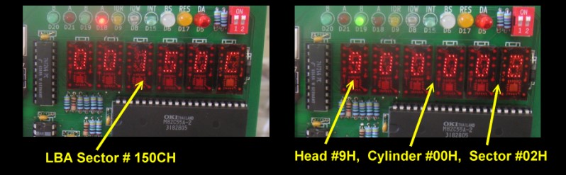
Download my “MYIDE.ASM” program to check things out. Run the program under CPM. The drive should come on and display the drive configuration parameters. See the picture above. The drive I used had 2082 cylinders, 16 heads and 63 sectors/track. You then need to read the sectors/track info you got and if required reassemble the program for your drive with the appropriate equates set in the software.
As I said, I have two of these new boards running here (on two systems).
They appear very reliable. I have extensively slopped large files to/from
memory disks and down to slow floppies. Never a problem. It’s so nice to
instantly have CPM3 boot up!
The only unusual thing I have found is the requirement of U4 being a fast
74H04 or 74S04 when using CF disks. It’s an absolute requirement for
the cards I have. Not so for regular hard disks. I have not really
determined why this is the case.
You can "Hot Swap" the CF cards in a running CPM system if you first turn off power to the IDE adaptor/CF board (SW3), remove the CF card. Insert the new card and THEN turn the power back on with switch SW3. With CPM you need to warm boot with a ^C. Clearly there must be a system on the new CF card or you must do the swap where another drive is the current system drive.
Software
.jpg)
AH = 02h
AL = number of sectors to read/written (must be nonzero)
CH = low eight bits of cylinder number
CL = sector number 1-63 (bits 0-5)
high two bits of cylinder (bits 6-7, hard disk only)
DH = head number
DL = drive number (bit 7 set for hard disk)
ES:BX -> data buffer
Because only 16 heads are allowed with this format, a hard disk can only get to 512MG in size. This is not a problem for 8 bit CPM systems since disk capacity was always less than 10 MG. To go to higher disk capacities with later version of MSDOS, the PC BIOS's utilized the so called "LBA" sector addressing mode. In this case sectors are numbered on the disk as just one long number. Starting at 0 and working upwards. There are no tracks or heads. Both formats can be implemented on our IDE board.
| Bit 7 | Bit 6 | Bit 5 | Bit 4 | Bit 3 | Bit2 | Bit 1 | Bit 0 |
| Always 1 | LBA/CHS mode | Always 1 | M/Slave | Heads 0-15 | |||
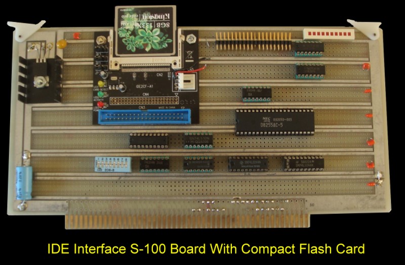
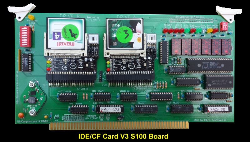
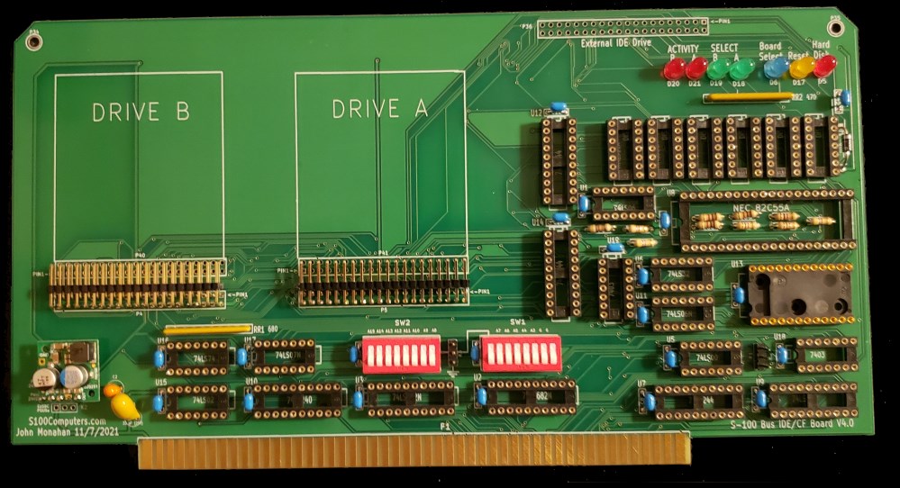
A Final Dual IDE
Prototype Board
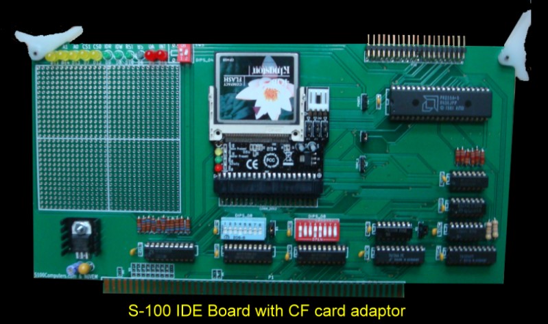
Utilizing all the observations above I constructed one more
prototype board to make sure everything is correct for what we expect will
be a popular S-100 board. Here is a picture of that board:-
.jpg)
Added where more LED's to let you know which CF card/drive is selected and
when a drive is active (RD/WR). The board works fine with 7403's rather than
the less common 74F03's. It also works fine with the low power CMOS 82C55's
or the older plain NMOS 8255's.
It is interesting to go back and see how this board has evolved.
It now has become a fairly sophisticated board and very useful.
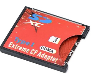
These days I store everything on CF cards!
Please note many older
S100 bus CPU boards do not set the S-100 bus upper 8 bits to zero for I/O port addressing. In this case jumper K5 2-3,
otherwise the CPU will not "see" the ports. (All S100Computers
boards use the upper 8 address lines for I/O port decoding). For I/O port address
00xxH, you need to close SW1 so the upper address lines will equate to low).
.jpg)
Source of chips
Most of the IC's use on this board are common 74LSxx chips available from
numerous sources such a Jameco, Mouser & DigiKey.
I did not want to change the basic 8255 driven circuit and all the software I and others have over the years written for the board. Sure if I were to do it all over again I would probably have done it different using perhaps a faster Zilog PIO or an onboard fast fully dedicated Z80 (as for our ZFDC board) or Propeller etc. The NEC or OKI 82C55-2’s are dirt common and seem to be able to handle anything the CPU sends to them.
I want to hand lay down broad power traces to all the boards IC’s for more even power distribution – particularly to the power hungry HEX displays.
I have inserted a trace “Keep out Area” on the front of the board so there is no danger of the IDE adaptors touching a critical trace.
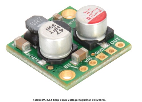
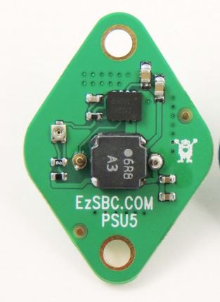
I have now switched to a “multi regular” voltage regulator footprint. This allows you to use either:- a 1.5Amp L7805CV, a TO-3 LM323K (3Amps), a Pololu 5 Volt , 2.5 Amp D24V25, or a EzSBC.com 3A regulator called PSU5.
I did bend the no new changes rules a little and added two 22V10 GALs. This greatly simplifies the board and really speeds up the port addressing and the potential drive select/reset issues some were having. I realize not everybody is familiar with GAL’s. Please see here for more information about GALs. The PALASM code is shown below. Again these GAL’s are fairly common (Jameco #39159 for the 15ns variety).
Correct the potential drive A: or B: switch circuit problem described above.
I have added a wait state circuit (0 - 8 I/O wait states) to accommodate very fast S100 boards such as our 80386 and 80486 boards without requiring further generalized I/O wait states on the CPU board for other system I/O ports.
People should be able to simply switch IC’s from the old board to this new one. Only two new GAL ICs and two 74LS373 are required.
Last but least I relabeled much of the Silk
Screen to be more relevant. For example placing IC numbers above their
pin locations etc.
 |
 |
 |
 |
 |
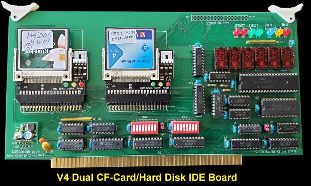
The board seems to be working fine with both CPM3 and MSDOS V4.01 with all our CPU's.
 |
 |
Damian Wildie noticed that the wait state circuit on the IDE/CF board was not functioning. He traced the issue to the GAL1 code which added a not pSYNC term to the address select, ADDR_8255 and ADDR_DR, equations. WAIT_SEL is derived from ADDR_8255 and ADDR_DR and is now only true when pSYNC is false. Since WAIT_SEL and pSYNC are handed by U106A, the load pulse for the wait state shift register U107 is never generated. He changed the WAIT_SEL equation
From: WAIT_SEL = ADDR_DR + ADDR_8255
 |
|
|
Bugs
There seems to be a problem
with the KiCad/Freerouter layout of this V4 board in that there are extra
traces to unused gates on the board. (I think a carry-over from earlier
versions). While a 'eye-sore" they do not in any way effect the
boards functionality. If somebody has a lot of free time on their
hands perhaps they could determine how the actual schematic differs from the
KiCAD one provided below.
CPM3 IDE/CF Card Download Images.
A Production S-100 Board
Realizing that a number of people might want to utilize a
board like this together with a group of
people on the
Google
Groups S100Computers Forum, a "group purchases" was formed. It is now closed.
Please see here
for more information. Please do not contact me directly.
The links below will contain the most recent schematic of the above boards.
Note, it may change over time and some IC part or pin numbers may not correlate
exactly with the text in the article above.
This page was last modified on 07/03/2022